LDO Definition
The Low dropout linear regulators or LDOs can be used in applications where you need to drop a higher input voltage to a lower output voltage at relatively moderate power levels. They are especially suitable in applications which require low noise, low current and which have a small difference between the input and output voltage.
LDO Features
LDOs regulate the output voltage by controlling the conduction of the pass element in a linear regulation. This linear regulation provides accurate, noise free output voltage which can quickly respond to load changes on the output. The key advantage of an LDO is its simplicity and low cost design with low noise and fast voltage conversion. However, compared to a switching regulator, an LDO has relatively low efficiency in applications with high VIN / VOUT ratio and power dissipation is more critical.
The linear regulation means that the voltage difference between input and output times the average load current is dissipated in the LDO pass element. Power Dissipation can be calculated as PD = (VIN - VOUT) * ILOAD, so big difference between VIN and VOUT with high load currents would lead to excessive dissipation. Higher power dissipation requires LDOs in larger packages, which increases cost, PCB space and application heat. When LDO power dissipation exceeds 0.8W, it is wise to look for alternatives such as Buck converters.
LDO regulators are typically used when:
- Converting a higher input voltage (VIN) into a lower output voltage (VOUT)
- A very clean power supply is required or when the application is noise sensitive
- The VIN/VOUT ratio is not very high, i.e. 3.3V to 2.5V
- The application draws moderate current (up to ~ 1A)
- The LDO power dissipation is limited, i.e. less than 0.8W
Applications
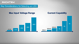
When selecting an LDO, one should first consider the input and output voltage range, the LDO current capability and package dissipation capability. LDO dropout voltage is the minimum VIN - VOUT voltage where the device can regulate.
In micro power applications, (i.e. applications that need to run from a battery for several years) the LDO quiescent current IQ needs to be low to avoid unwanted battery drain. These applications need special low IQ LDOs. In applications that require a very clean and low noise output voltage, low noise and good PSRR will be the LDO key selection criteria.
In order to select a right LDO for your application, some key criteria are important to be considered: Fixed or adjustable output voltage, output current, power dissipation & package selections, dropout voltage, PSRR, and quiescent current.
VOUT
Do you need an adjustable output voltage? Which method do you prefer?
Fixed output voltage LDOs have the feedback network internally. Adjustable output LDOs use an external feedback network, which gives more flexibility. Some adjustable parts also have an internal feedback network, so they can be used as fixed output version as well.
IOUT
What is the current requirement of your application?
The current capability relates directly to dropout voltage and power dissipation. For larger current capability, please select LDO controllers with external MOSFETs.
Power Dissipation
What is the current requirement of your application?
The power dissipation in the LDO is determined by the voltage drop (VIN-VOUT) across the LDO multiplied by the current passing through the LDO (IOUT), which can be calculated from the formula
PD = (VIN - VOUT) * ILOAD.
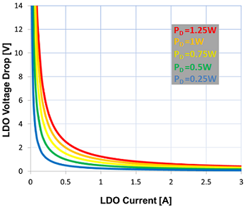 The right graph shows the allowed LDO voltage drop versus LDO current for specific power dissipation values. Larger current or larger voltage drop across the LDO quickly leads to high device power dissipation. The LDO package needs to be able to handle this power dissipation.
Maximum allowed device power dissipation for SMD type LDOs depends on package, PCB layout and ambient temperature. You can calculate the allowed power dissipation by dividing the allowed temperature difference between junction and ambient by the thermal resistance between junction and ambient. The thermal resistance value θJA is shown in the datasheet, but keep in mind that this value is based on the JEDEC method, which can be slightly conservative.
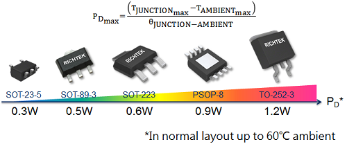
Here are some practical power dissipation limits for various package types, based on a normal PCB layout with some extra copper connected to the package pins and thermal pad, a maximum PCB ambient temperature of 60°C, and maximum silicon die temperature of 125°C. If your ambient temperature is lower, the power dissipation can be higher. If your PCB is small, or there are other hot components nearby, the maximum power dissipation may be less.
Learn more about improving your thermal design in our tutorial video.
Dropout Voltage
LDOs need a certain minimum voltage drop to regulate correctly.
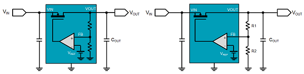
LDOs are Low Dropout Linear regulators. It basically means that these devices can still regulate the output voltage, even when the input voltage is very close to the output voltage. LDO dropout voltage is defined as the voltage drop across the regulator where the device can no longer regulate the output voltage.
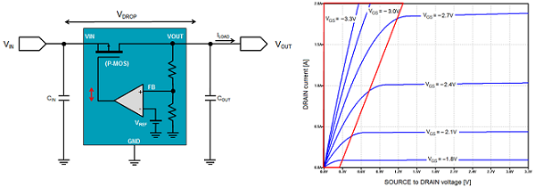
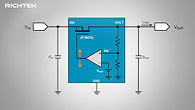
Here is the basic circuit of an LDO with a P-channel MOSFET pass device. The MOSFET source is connected to VIN. To regulate the output voltage, the error amplifier controls the P-MOSFET gate voltage with respect to VIN, thereby controlling the MOSFET conduction level. The LDO needs a certain amount of input to output voltage difference for regulation.
When the difference between input and output voltage becomes smaller, the MOSFET operation shifts toward the MOSFET Ohmic region toward the left in the MOSFET I/V curves. In the Ohmic region, the MOSFET becomes resistive, and the error amplifier will pull the gate near ground level. At that point, the output voltage cannot be regulated anymore.
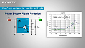
PSRR
If your device is sensitive to supply ripple and noise, a low noise linear regulator is an ideal choice for this supply.
PSRR stands for power supply ripple rejection. The LDO PSRR value quantifies how well the LDO can reject input supply ripple at a certain frequency to keep the output voltage free of noise and ripple. In Richtek datasheets, PSRR is defined as the ripple attenuation ratio VOUT/VIN, therefore lower PSRR values are better.
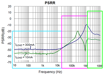
The diagram shows the example of PSRR vs. frequency. At frequencies up to 10kHz, LDOs have high open loop gain, and can reject input ripple very well.
When frequency increases, the loop gain reduces due to the bandwidth limit of the LDO, and the PSRR curves rise. Higher LDO load pushes the load pole upwards, so the unity gain frequency at high load is also higher. In this example the LDO unity gain frequency is 300kHz at light load and 1MHz at high load, as can be seen from the peaks in the graph.
Above the unity gain frequency, the LDO is not able to actively remove ripple. The ripple attenuation at these very high frequencies is mostly caused by the LDO output capacitor and the LDO internal parasitic impedance.
Learn more about LDO PSRR and practical design tips for using a LDO as a ripple and noise filter in our tutorial video.
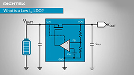
Ultra Low Quiescent Current
(IQ)
Does your application need to run from a small battery cell for
long periods?
These applications often will run in sleep mode most
of the time, and are only active for short periods. To minimize
the power consumption in sleep mode, you need to select parts with
very low quiescent current, and this is where Richtek ultra low
IQ LDOs are really suitable.
The LDO quiescent current is the current that is consumed by the IC internal feedback control and drive circuits. It is normally measured by measuring the current that flows out of the LDO ground pin.
The Richtek Low IQ LDO portfolio contains LDOs with quiescent currents down to 1µA, which extends battery lifetime considerably.
Richtek ultra low IQ LDOs
provide dynamic quiescent current control for obtaining the best performance
in battery powered applications requiring long battery life and good
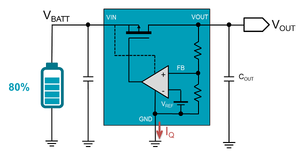
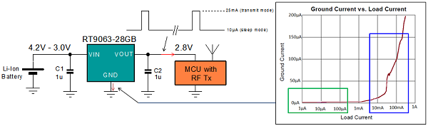
dynamic load performance. The Low IQ LDO RT9063 provides
a stable 2.8V supply to the micro controller, and the LDO ground current
stays relatively constant at 1µA in the low load range, thereby prolonging
battery life.
But at higher load currents, the ground current increases to improve the dynamic behavior of the LDO; when a sudden high load is encountered, the internal control circuit uses more energy to ensure a tight regulation of the output voltage.
Find out more in our
tutorial video.
Videos
LDO Introduction
Low dropout basically means that the LDO can still regulate the output voltage, even when the input voltage is very close to the output voltage. But what is the difference between a PMOS type LDO and a NMOS type LDO? Why is it better to choose a NMOS type LDO for applications with Vin lower than 2.5V? In which applications can an LDO replace a Buck converter? Find out more here.
Power Dissipation
To get the most out of your LDO application, the LDO power dissipation needs to be carefully considered. The power dissipation in the LDO is determined by the voltage drop across the LDO multiplied by the current passing through the LDO. Increasing the LDO voltage drop or the LDO current quickly leads to higher dissipation. But how much power can you dissipate in the LDO? Learn more about package power dissipation and how to improve your thermal design in the video.
Dropout Voltage
LDOs are Low Drop-Out Linear regulators. But what exactly does Low Dropout mean? How well does an LDO regulate the output voltage when the input voltage is very close to the output voltage? Our video will explain the LDO dropout operation and dropout curves, and gives a practical measurement example of the RT9187 LDO close to dropout operation.
PSRR
If your application requires a supply voltage that is free of ripple and noise, you may want to use an LDO as voltage regulator. But how well can an LDO remove ripple and noise from an input supply rail? This is related to the LDO Power Supply Ripple Rejection (PSRR). Find out about PSRR vs. frequency and practical design tips for using a LDO as a ripple and noise filter in the video.
Ultra Low Quiescent Current
Learn why Richtek ultra low IQ LDOs use dynamic quiescent current control for obtaining the best performance in battery powered applications requiring long battery life.